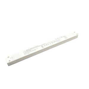
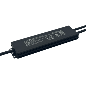
Just how advanced is the chip technology in LED dimming power supplies?
The evolution of LED lighting has been profoundly shaped by breakthroughs in semiconductor engineering, particularly within the compact yet potent chips embedded in dimming power supplies. These tiny silicon marvels now govern everything from color temperature transitions to millisecond-responsive brightness adjustments—capabilities unimaginable a decade ago when basic PWM (Pulse Width Modulation) dominated the market. Today’s high-end solutions leverage multi-layered architecture combining digital signal processors with analog front ends, creating hybrid systems that marry mathematical precision with real-world adaptability.

At the heart lies programmable microcontroller units (MCUs) executing complex firmware routines. Unlike legacy designs relying on fixed resistor networks, contemporary chips dynamically calculate optimal duty cycles based on ambient light sensors and user preferences. Advanced models incorporate fuzzy logic algorithms to eliminate perceptible flicker during low-range dimming—a critical improvement for cinematic applications where consistent illumination below 1% rated output was previously unattainable. Manufacturers like Texas Instruments and STMicroelectronics have pioneered neural network accelerators directly onto these chips, enabling machine learning-driven predictive dimming patterns that anticipate environmental changes before they occur.
Power factor correction represents another leap forward. Modern ICs achieve near-unity power factors across all load levels through quasi-resonant topologies, slashing harmonic distortions while recovering typically 15–20% more usable energy compared to linear regulators. This isn't merely theoretical efficiency; field tests show commercial installations reducing annual electricity bills by up to $370 per thousand fixtures after retrofitting with upgraded drivers featuring nextgen TMS320 series DSP cores.
Thermal management innovations deserve equal attention. Engineers now implement thermal foldback protection at the chip level—automatically throttling output when PCB temperatures exceed safe thresholds—without sacrificing performance. Companies such as OnSemi conduct accelerated life testing simulating ten years of operation within seventy-two hours using specialized climatic chambers linked directly to their ASIC development platforms. Such rigor ensures compliance with IEC 62384 standards while pushing operational limits beyond traditional boundaries.
Wireless integration further demonstrates technological maturity. Bluetooth Low Energy modules shrink enough to coexist alongside primary controllers on single substrate layers, allowing smartphones or voice assistants to fine-tune lighting scenes with sub-millisecond latency. More sophisticated protocols like Zigbee Pro even support mesh networking across hundreds of nodes, transforming entire buildings into responsive ecosystems where each fixture acts as both sensor and actuator.
Perhaps most impressive is how miniaturization hasn't compromised functionality. Through advanced packaging techniques including system-in-package (SiP) modules, designers cram AC/DC conversion stages alongside intelligence layers into footprints smaller than postage stamps. Yet despite diminutive size, these powerhouse components handle surge currents exceeding 50A during startup sequences—a testament to wide bandgap semiconductor materials replacing older silicon carbide composites.

As industry moves toward GaN FET replacements and gallium oxide substrates promise even greater conductivity gains, one truth emerges clearly: the humble chip inside your LED driver has become an extraordinary convergence point where materials science meets computational genius. No longer just switches controlling current flow, they’ve evolved into intelligent hubs orchestrating light’s interaction with human perception, architectural spaces, and global energy grids alike.
 In heritage architecture prote
 When small-batch customization
 Have the electromagnetic emiss
 When Triac dimmable power supp
